Researchers developing window coating with variable light absorption
February 3, 2017
By
CCE
The material is capable of absorbing light from every angle, and it also can theoretically be customized to absorb certain wavelengths of light while letting others pass through.

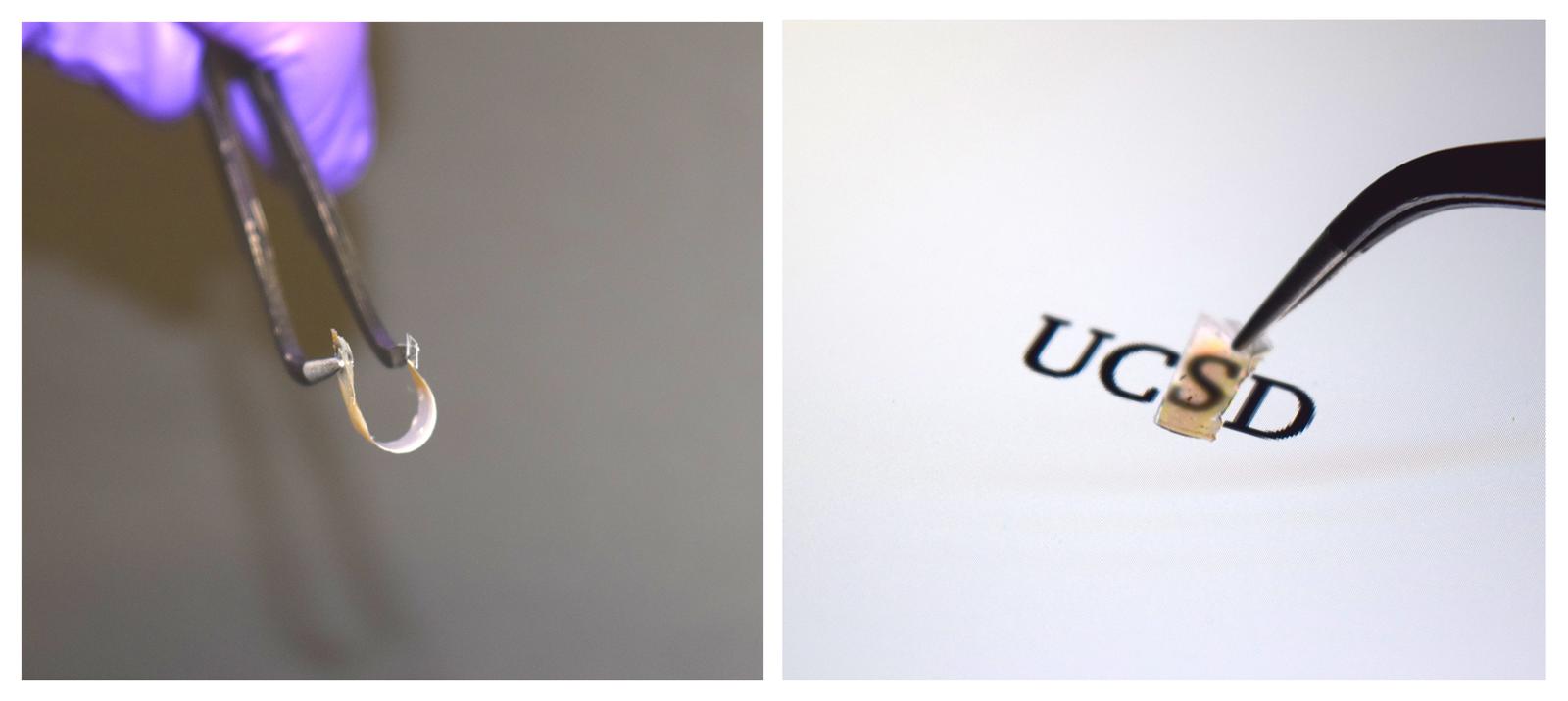
Broadband absorber that’s thin, flexible and transparent in visible light (source: UC San Diego, Jacobs School of Engineering)
Engineers at the University of California San Diego are working on a thin, flexible, light-absorbing material that could work as a transparent window coating to keep buildings cool and could also work on devices that could more than triple solar cell efficiencies.
The material, being called a near-perfect broadband absorber, absorbs more than 87 per cent of near-infrared light (1,200 to 2,200 nanometer wavelengths), with 98 per cent absorption at 1,550 nanometers, the wavelength for fiber optic communication.
The material is capable of absorbing light from every angle, and it also can theoretically be customized to absorb certain wavelengths of light while letting others pass through.
The nanoparticle-based design, led by professors Zhaowei Liu and Donald Sirbuly at the UC San Diego Jacobs School of Engineering, creates a broadband absorber that’s thin, flexible and tunable. Their work was published online on Jan. 24 in Proceedings of the National Academy of Sciences.
“This material offers broadband, yet selective absorption that could be tuned to distinct parts of the electromagnetic spectrum,” Liu said in a release from UC San Diego.
The release explains that the absorber relies on optical phenomena known as surface plasmon resonances, which are collective movements of free electrons that occur on the surface of metal nanoparticles upon interaction with certain wavelengths of light. Metal nanoparticles can carry a lot of free electrons, so they exhibit strong surface plasmon resonance—but mainly in visible light, not in the infrared.
The engineers reasoned that if they could change the number of free electron carriers, they could tune the material’s surface plasmon resonance to different wavelengths of light. “Make this number lower, and we can push the plasmon resonance to the infrared. Make the number higher, with more electrons, and we can push the plasmon resonance to the ultraviolet region,” Sirbuly said. The problem with this approach is that it is difficult to do in metals.
To address the challenge, engineers designed and built an absorber from materials that could be modified to carry a different amount of free electrons: semiconductors. Researchers used a semiconductor called zinc oxide, which has a moderate number of free electrons, and combined it with its metallic version, aluminum-doped zinc oxide, which houses a high number of free electrons — not as much as an actual metal, but enough to give it plasmonic properties in the infrared.

SEM images of a nanotube array: side view (left) and top view (right): (source: UC San Diego, Jacobs School of Engineering)
The materials were combined and structured in a precise fashion using advanced nanofabrication technologies. The materials were deposited one atomic layer at a time on a silicon substrate to create an array of standing nanotubes, each made of alternating concentric rings of zinc oxide and aluminum-doped zinc oxide. The tubes are 1,730 nanometers tall, 650 to 770 nanometers in diameter, and spaced less than a hundred nanometers apart. The nanotube array was then transferred from the silicon substrate to a thin, elastic polymer. The result is a material that is thin, flexible and transparent in the visible.
“There are different parameters that we can alter in this design to tailor the material’s absorption band: the gap size between tubes, the ratio of the materials, the types of materials, and the electron carrier concentration. Our simulations show that this is possible,” said Conor Riley, a recent nanoengineering Ph.D. graduate from UC San Diego and the first author of this work. Riley is currently a postdoctoral researcher in Sirbuly’s group.
The particle-based design is potentially transferrable to any type of substrate and can be scaled up to make large surface area devices, like broadband absorbers for large windows. “Nanomaterials normally aren’t fabricated at scales larger than a couple centimeters, so this would be a big step in that direction,” Sirbuly said.
The technology is still at the developmental stage. Liu and Sirbuly’s teams are continuing to work together to explore different materials, geometries and designs to develop absorbers that work at different wavelengths of light for various applications.